Manufacturers of semiconductor components repeatedly report on the benefits of vias for heat dissipation, also called thermal via: Thermovias are mechanically drilled vias from TOP to BOTTOM. Ideally, vias are placed directly under the components and exclusively intended for heat dissipation.
Usually, Manufacturers provide general recommendations for guidance respectively ideal dimensions and distances of these thermovias. However, these guidelines, mostly referring to the demoboard of the respective manufacturer, do not consider the fact that in this way no generally valid statement can be made for all designs. The design of the board and its size as well as the number of layers affect the validity of the recommendations quite substantially. So, the decision concerning the number of thermovias should always be made on an individual basis. Furthermore, it should be taken into account that a larger number of thermovias cannot “dissipate” more heat, even though time and costs increase proportionally. Instead, it is more important to find a appropriate number of vias which balances benefits and costs.
This raises the question: How do you obtain a result that really works for your printed circuit board? How many thermal vias are practically feasible in terms of manufacturing effort and costs?
The experimental effort needed to determine the ideal number for any given design would be excessive. Excel sheets that “calculate” the thermal resistance of n-pieces of thermal via would be even impractical. Merely a simulation program can provide a meaningful graph for temperature vs. number of holes in a short time at low cost.
PCB-Investigator Physics is a simulation tool that is able to reproduce the design status of any circuit board in detail and therefore allows you to explore the possibilities of thermal vias. The layer stackup, the schematic and the drilling scheme are imported from ODB++/IPC2581 data and can subsequently be used for the thermal simulation. Both vias and plated micro vias can be used for the drilling process. In addition, thermal data such as the thermal conductivity of FR4, the temperature and the state of motion of the surrounding air are required – with Physics all parameters can be set and adjusted in a few minutes. If you play around with the pitch, number and arrangement of the thermovias, you can predict a reasonable prototype that will not cause any problems in production regarding its thermal behavior.
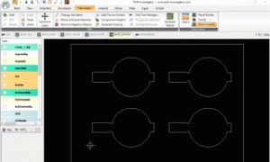
Let us illustrate these deliberations by using a concrete example. In a 2-layer board (Fig. 1) there is a heat-critical component. We wish to control the temperature of this component with the help of thermal vias and/or cause a reduction in temperature.

Fig. 1: Example for the thermal analysis with PCB-Investigator Physics. Thermal vias will be drilled under the large black IC to ensure improved heat dissipation.
For simplification, a basic layer stack-up was chosen. However, there are no restrictions when using PCB-Investigator regarding potential multilayer boards.
The simulation program PCB-Investigator Physics automatically creates a physical calculation model based on the geometry data, which takes into account both the heat conduction within the board and the heat transfer to the ambient air. As for all 3D field solvers, the calculation time will vary depending on the number of nodes and the convergence speed, as the calculation is transferred in an iterative loop from cold to heated state. To speed up the computation, PCB-Investigator Physics uses the graphics processor (GPU) to increase the time per iteration significantly in comparison to the CPU. Reliable results can thus be delivered in just a few minutes.
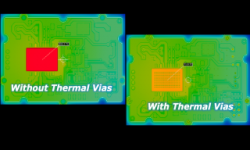
The simulation result for the sample board without thermovias is shown in Fig. 3. The temperature of the component is 103.4°C without vias.

Fig. 3.1: Simulation results (3D) of the printed circuit board without thermovias.


Fig. 3.2: Simulation result of the top side (102.1°C) and bottom side (65.5°C) without any microvias.
Using 15 thermal vias arranged in a regular pattern, the following image emerges (Fig.4.). The temperature of the component is substantially lower due to the heat dissipation of the vias, reaching 83.9°C.

Fig. 4.1: 3D view of the circuit board with 15 thermovias. The orange color of the component indicates a considerable cooling of the component.


Fig. 4.2: Simulation result of the top side (82.0°C) and bottom side (69.1°C) with 15 thermovias (visible as green dots).
Besides the thermal vias, there are also other factors that play a decisive role for heat dissipation and must therefore be included in the thermal management considerations of the PCB. On the one hand, heat tends to flow into well-conducting materials, i.e. the traces, and on the other hand the heat can hardly skip the FR4 pitches between the traces (of course there is heat transport in the FR4, which is even considerable due to its volume and area). The reduction of the component temperature from about 103°C to 84°C is already enormous, especially with respect to the ambient temperature (20°C).
Let’s add some more thermal vias to the simulation (Fig.5) and see the resulting heat dissipation.

Fig. 5.1: View of the printed circuit board (3D) with 170 holes.


Fig. 5.2: Simulation result of the top side (71.5°C) and bottom side (70.6°C) with 170 thermovias (visible as green dots).
The multiplication of the thermal vias has led to a considerable reduction in temperature here. The temperature of the component has now reached 72.8 °C, a reduction of about 30 °C due to a better heat dissipation.
Now, the question arises about the usefulness of further drillings, after we could already achieve such a strong cooling. However, at a certain point we can see that some kind of saturation is reached at which the temperature curve flattens out steadily, although the number of thermal vias is increased to an even greater extent. Thus, if the number of vias is quadrupled to a total of 680, a relatively small reduction in temperature to 72°C is observed, corresponding to a cooling of less than 1°C. The temperature of the bot layer is almost identical to the one of the top layer. As a result, further heat dissipation is no longer possible.
It can be concluded that at a certain number of thermal vias the utility will become less than the expense, meaning that the design should not simply be arbitrarily designed with as many drill holes as possible.
You can see this effect in the following diagram (Fig 6). It shows an increasing approximation of the graphs of the bot and top layer with regard to their maximum temperature as a function of the amount of thermal vias. Likewise, an increasing flattening of the temperature curve can be noted despite the increasing number of vias. The decline in temperature reaches the aforementioned saturation. It is caused by the convection flow on the surface of the PCB which represents a terminating thermal resistance. That resistance is unaffected by the number of thermal vias and cannot be undercut; a fan or heat sink would have to be used to lower it.

Fig. 6.1: Overview of the temperature variations depending on the quantity of thermal vias.

Fig.6.2: Parameter study. Even with an infinite number of thermovias, the component will not be colder than about 70 °C.
Depending on the application of your board, the intended housing and the expected ambient temperature, different temperature limits must be observed. These limits should be calculated preferably at the design stage of the board to avoid late and expensive modifications caused by the lack of thermal management.
PCB-Investigator Physics enables you to determine the ideal number of thermal vias for your design so that given temperature limits are not exceeded. At the same time, you can avoid additional costs and time delays caused by additional but unnecessary vias. Find out how many thermal vias your board actually needs!
Using Physics simulation, thermal vias can be planned in a time- and cost-saving way.