Create a comprehensive overview of your PCB development with the Design Report in PCBI!

This unique plug-in on the CAD/CAM market provides an overview of all the important parameters of a printed circuit board.
Such an overview is especially useful in collaboration with others involved in the development and production process, as it streamlines workflows and eliminates the need for constant follow-up questions.
Since the Design Report is generated as a Word document, it can also be edited later by adding the company name and address, for example.
The following points are automatically generated by the plug-in and can be supplemented with the results of various analyses (for example, the Component Analysis plug-in).
- Number of steps
- Camp names
- Net names
- Components and pins
- Information about the layer structure
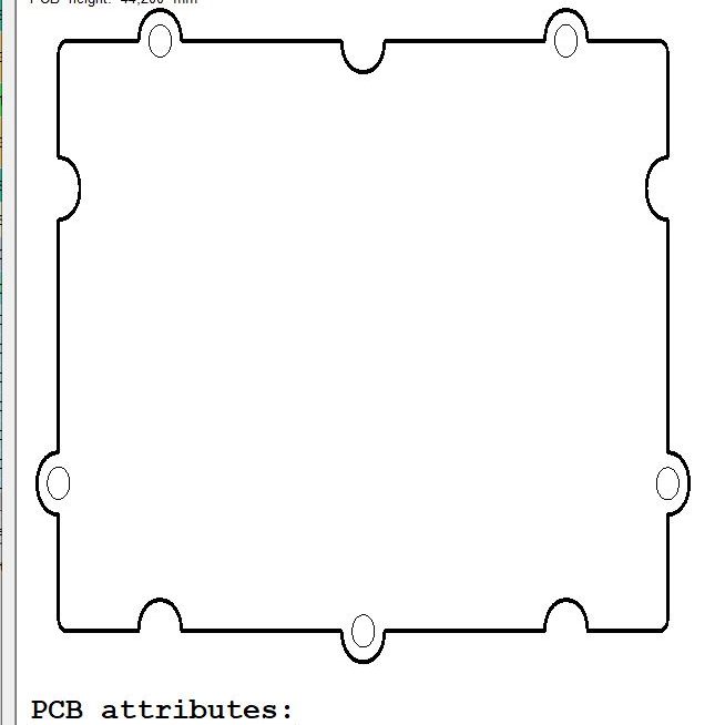
- Size of the printed circuit board with an outline sketch
- Number of drills and size of the smallest drill
After that, the report can also be exported as RTF.


