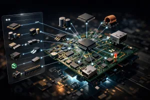
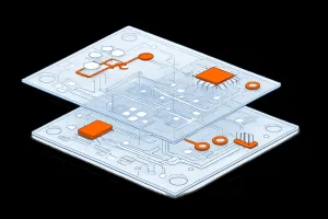
- Thermal Simulation for PCB Layout and Current Flow
 See thermal risk before the first prototype In PCB design, the most expensive problems are often the ones you only discover after fabrication. Local overheating, excessive current density, or unacceptable voltage drop can all remain hidden until late verification. PCB-Investigator… Read more: Thermal Simulation for PCB Layout and Current Flow
 - PCB Design Report for Faster Reviews and Handoffs
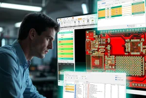
 Turn scattered PCB data into a clear design report In many PCB projects, the critical information is already there — it is just spread across CAD data, analysis results, and repeated questions from different teams. The Design Report in PCB-Investigator… Read more: PCB Design Report for Faster Reviews and Handoffs
 - Improve PCB Analysis with Net Groups
 Analyze smarter by grouping related nets In PCB development, speed and consistency matter just as much as accuracy. That is exactly where Net Groups help: they bundle logically related nets into a structured group, making complex design analysis easier to… Read more: Improve PCB Analysis with Net Groups
 - Tombstone DFM Analysis for Safer SMT Designs
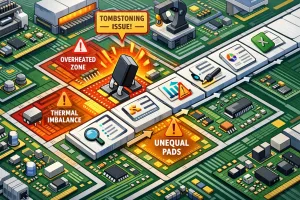 Catch tombstone risk before reflow does Tombstone defects are a classic SMT manufacturing issue: a small component lifts on one end and stands upright after reflow, typically affecting resistors or capacitors. The root cause is often uneven heating or an… Read more: Tombstone DFM Analysis for Safer SMT Designs
 - PCB Tools That Surface Risk Before It Escalates
 The best PCB tools do not just answer questions They help engineers ask the right ones. That is the real difference between a simple viewer and a true analysis platform in electronics development. The challenge is usually not a lack… Read more: PCB Tools That Surface Risk Before It Escalates
 - Machine Formats for Smarter PCB Manufacturing
 Making PCB data move cleanly into production In PCB manufacturing, design quality is only part of the equation. The other part is how reliably your data reaches the machines that need it. PCB-Investigator supports a wide range of machine formats… Read more: Machine Formats for Smarter PCB Manufacturing
 - The Most Expensive PCB Errors Start in Layout
 Late detection is what makes PCB errors expensive The most costly PCB defects are often not created on the production line. They start weeks earlier in the layout phase, where a missing clearance, a forgotten drill tolerance, or a poorly… Read more: The Most Expensive PCB Errors Start in Layout
 - PCB Design Report for Faster Engineering Workflows
 Why a PCB Design Report matters In PCB development, critical information is often scattered across layout data, analysis results, manufacturing notes, and team communication. The Design Report in PCB-Investigator brings that information together in a structured overview of the most… Read more: PCB Design Report for Faster Engineering Workflows
 - DFM Analysis for More Reliable PCB Manufacturing
 Catch manufacturing issues before the first board is built Design for Manufacturing is not a late-stage checklist. It is one of the most effective ways to reduce assembly risk, avoid rework, and improve overall product quality before the board ever… Read more: DFM Analysis for More Reliable PCB Manufacturing
 - PCB-Investigator Manual for Faster PCB Analysis
 A better starting point for PCB-Investigator When you work with complex PCBs, software capability alone is not enough. You also need documentation that helps engineers move quickly from question to answer, and that is exactly what the PCB-Investigator Manual is… Read more: PCB-Investigator Manual for Faster PCB Analysis
 - Fast Impedance Calculation for High-Speed PCB Design
 Keep impedance under control in high-speed PCB designs As data rates rise and edge speeds get faster, controlled impedance becomes a design constraint rather than a nice-to-have. Even small deviations in trace geometry, layer stackup, or material properties can affect… Read more: Fast Impedance Calculation for High-Speed PCB Design
 - Smarter PCB Panelization with Panel Builder
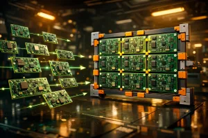 Panelization should not slow down your fabrication flow Anyone responsible for preparing PCB designs for manufacturing knows the pressure: layouts must be arranged into panels, spacing rules must be respected, fiducials need to be placed correctly, and internal fabrication constraints… Read more: Smarter PCB Panelization with Panel Builder
 - We’re excited to announce the release of PCB-Investigator V17.1!
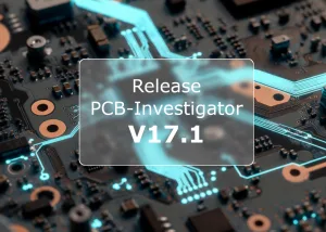 This update builds on the strong foundation of V17 and brings a wide range of improvements across AI & automation, analysis, import/export, data management, and the user interface — making your PCB workflows smarter and more efficient than ever. What… Read more: We’re excited to announce the release of PCB-Investigator V17.1!
 - PCB-Investigator Training for Every Skill Level
 Training that matches real engineering needs Whether you are just getting started with PCB-Investigator or already use PCB analysis tools every day, the right training makes a measurable difference. It shortens the learning curve, reduces trial-and-error, and helps teams apply… Read more: PCB-Investigator Training for Every Skill Level
 - Efficient PCB Change Tracking with Database Compare
 Make PCB change tracking faster and more reliable In PCB development, change tracking is not a side task. It is a critical part of the workflow, especially during design reviews where layout updates, net changes, and component revisions must be… Read more: Efficient PCB Change Tracking with Database Compare
 - Validate AOI Inspectability Before Production Starts
 AOI problems usually start in the layout If an automated optical inspection system cannot see a pin, the root cause is often not the line—it is the PCB design. Tight component spacing, unfavorable viewing angles, or hidden pins can force… Read more: Validate AOI Inspectability Before Production Starts
 - PCB-Investigator: 30-Day Free Trial for Engineers
 PCB-Investigator: 30-Day Free Trial for Engineers Choosing PCB analysis software is never just about features on a product page. The real question is whether the tool fits your engineering workflow, your review process, and your technical requirements. That is exactly… Read more: PCB-Investigator: 30-Day Free Trial for Engineers
 - Stencil Analysis for Better PCB Manufacturing Quality
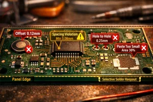
 Why Stencil Analysis Matters in PCB Development In PCB manufacturing, success is not determined by the circuit layout alone. Just as important is whether the solder paste areas are properly designed to support reliable assembly and clean reflow results. That… Read more: Stencil Analysis for Better PCB Manufacturing Quality
 - Power Pin Wizard for Faster PCB Power Net Review
 See power and ground connections instantly In complex PCB layouts, quickly identifying the most important supply and ground connections can save a surprising amount of time. The Power Pin Wizard in PCB-Investigator highlights power and GND pins directly in the… Read more: Power Pin Wizard for Faster PCB Power Net Review
 - Tutorial: DRC Analysis with PCB Investigator – Detect Manufacturing Issues Early
 Every PCB design contains potential risks that may only become apparent during manufacturing—such as insufficient trace spacing, inadequate annular rings, solder mask clearance issues, or critical drill-to-copper distances. With PCB Investigator’s Bare Board Analysis (DRC), these issues can be identified… Read more: Tutorial: DRC Analysis with PCB Investigator – Detect Manufacturing Issues Early
 - PCB 3D Export for STEP, OBJ, PDF and WebGL
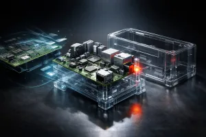 From PCB layout to usable 3D data When PCB development meets mechanical design, 2D data is often not enough. Housing checks, assembly reviews, and ECAD-to-MCAD handoffs become much easier when the board can be evaluated in a 3D context. PCB-Investigator’s… Read more: PCB 3D Export for STEP, OBJ, PDF and WebGL
 - PCB-Investigator License Models Compared
 Which license model fits your engineering team? When deploying engineering software, the license model often determines how smoothly the tool will be used in daily work. PCB-Investigator offers three different licensing options: SOD (Software on Demand), Floating licenses, and dongle-based… Read more: PCB-Investigator License Models Compared
 - How Much Knowledge Is Hidden in Your PCB Data?
 More Than Geometry In many projects, PCB data is treated primarily as the foundation for layout work. But a closer look reveals that these files contain far more than traces and pads. Net structures, component information, test points, spacing, layer… Read more: How Much Knowledge Is Hidden in Your PCB Data?
 - Virtual BOM Export for Visual PCB Collaboration
 When a BOM needs to do more than list parts In many projects, the BOM is still treated as a static document. The data may be correct, but the crucial context is missing: where each component sits on the PCB… Read more: Virtual BOM Export for Visual PCB Collaboration
 - Find PCB Problems Before They Hit Production
 Many PCB issues are already visible before fabrication Some of the most expensive PCB problems are not manufacturing surprises at all—they are already present in the data long before the first board is built. That makes early analysis one of… Read more: Find PCB Problems Before They Hit Production
 - Testpoint Report for Faster PCB Testpoint Analysis
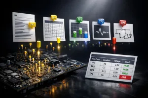 Make testpoint management easier Testpoint administration is one of those tasks that can quietly consume time in PCB projects. The Testpoint Report in PCB-Investigator is designed to bring structure and clarity to that process, helping engineering teams analyze testpoints more… Read more: Testpoint Report for Faster PCB Testpoint Analysis
 - Hazard Analysis for Safer PCB Layouts
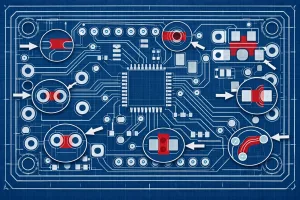 Catch layout hazards before they become failures In PCB design, minimum clearance is not a detail you can leave to the end of the process. If conductive features sit too close together, you risk leakage currents, short circuits, and costly… Read more: Hazard Analysis for Safer PCB Layouts
 - Component Connection Analysis for PCB Verification
 Clearer visibility at pin and net level Reliable production starts with traceable analysis. The Component Connection Analysis Plug-in in PCB-Investigator examines every pin connection of a selected component and displays the associated net names and lengths. For engineers, PCB designers,… Read more: Component Connection Analysis for PCB Verification
 - PCB-Investigator DRC for PCB Manufacturability Checks
 DRC analysis that catches fabrication problems early In PCB design, the board may look perfect in CAD and still create costly questions in fabrication. That is exactly where the Design Rule Check (DRC) in PCB-Investigator adds value: it validates manufacturability… Read more: PCB-Investigator DRC for PCB Manufacturability Checks
 - Edit Components for Faster PCB Layout Changes
 PCB component editing should not slow down design iteration In PCB development, the biggest delays are often not in routing itself, but in the steps around it: checking placement, refining component positions, and keeping libraries aligned with design reality. That… Read more: Edit Components for Faster PCB Layout Changes
 - Creepage Analysis for Safer PCB Layouts
 Validate safety distances before they become a problem As soon as a design crosses the 30 V threshold, creepage becomes a real engineering concern. At that point, it is no longer enough to estimate spacing visually; you need to verify… Read more: Creepage Analysis for Safer PCB Layouts
 - Component Analysis for Smarter PCB Manufacturing
 Catch assembly risks before they reach production In PCB manufacturing, the expensive problems are often introduced long before the board reaches the line. Critical component spacing, height-related constraints, and challenging placements can all affect solderability, assembly flow, and downstream testability.… Read more: Component Analysis for Smarter PCB Manufacturing
 - Package Expert: Realistic Component Bodies for PCB Analysis
 Why geometry quality defines the value of PCB analysis Many PCB analyses depend entirely on the quality of the underlying geometric data. In practice, CAD packages are often oversized, inconsistently modeled, or inconsistent across designs and customers. The result: clearance,… Read more: Package Expert: Realistic Component Bodies for PCB Analysis
 - Fabrication Edition for Predictable PCB Production
 Catch production issues before the first board is made In PCB manufacturing, the difference between a smooth launch and an expensive delay is often determined long before the first board hits the line. With the PCB-Investigator Fabrication Edition, production planners,… Read more: Fabrication Edition for Predictable PCB Production
 - PCB-Investigator Developer for PCB Design Review
 From design review to production readiness Modern PCB development is no longer just about visual inspection. If you want to deliver robust, production-ready boards, you need tools that reveal critical details, keep changes traceable, and support efficient validation workflows. That… Read more: PCB-Investigator Developer for PCB Design Review
 - PCB-Investigator Physics for Early Thermal Analysis
 Catch thermal issues before the first prototype Thermal problems are among the most expensive surprises in PCB development. If hotspots, critical trace resistance, or unexpected voltage drops only appear after fabrication, teams lose time, budget, and often momentum. The Physics… Read more: PCB-Investigator Physics for Early Thermal Analysis
 - PCB-Investigator Ultimate for End-to-End PCB Workflows
 One edition for development, analysis, and production readiness PCB teams rarely work in a straight line. Design decisions, manufacturing constraints, verification tasks, and documentation requirements all overlap, and that is exactly where PCB-Investigator Ultimate is positioned. It combines the functionality… Read more: PCB-Investigator Ultimate for End-to-End PCB Workflows
 - 3D Export for PCB Design: STEP, OBJ, PDF and WebGL
 Turn PCB layouts into usable 3D models In many development projects, the ECAD/MCAD handoff starts with the same challenge: the PCB layout is ready, but mechanical engineering needs a 3D model they can actually work with. This is exactly where… Read more: 3D Export for PCB Design: STEP, OBJ, PDF and WebGL
 - PCB Impedance Calculation Made Faster and Safer
 Why impedance checks belong early in PCB design As data rates rise and edge speeds get faster, impedance control becomes a core design task rather than a final verification step. For high-frequency traces, even small changes in geometry, stack-up, or… Read more: PCB Impedance Calculation Made Faster and Safer
 - PCB-Investigator Production Control for PCB Manufacturing
 Connecting design and production in one continuous workflow In PCB manufacturing, data handoff is often the hidden source of delays, errors, and unnecessary cost. The Production Control Edition of PCB-Investigator is designed to close that gap by connecting design and… Read more: PCB-Investigator Production Control for PCB Manufacturing
 - PCB-Investigator Basic for Efficient PCB Review
 PCB design review without unnecessary complexity In PCB development, the best tool is not always the one with the most features. It is the one that helps engineers review designs quickly, clearly, and without distractions. PCB-Investigator Basic is built exactly… Read more: PCB-Investigator Basic for Efficient PCB Review
 - Stencil Analysis for Better PCB Manufacturing Quality
 Why stencil analysis matters in PCB production In PCB manufacturing, small details often determine whether a build runs smoothly or creates avoidable quality issues. Insufficient paste coverage or an unfavorable relationship between stencil thickness and paste deposition can affect assembly… Read more: Stencil Analysis for Better PCB Manufacturing Quality
 - BOM Expert for Faster PCB AVL and Parts Verification
 Why BOM verification deserves more attention In PCB development, the bill of materials is not just an administrative file. It is a technical control point that influences sourcing, assembly accuracy, manufacturability, and the quality of the final digital twin. When… Read more: BOM Expert for Faster PCB AVL and Parts Verification
 - Visual PCB Revision Compare with Graphic Board Compare
 Why precise PCB comparison matters in development In PCB engineering, small design changes can have a major impact on manufacturability, quality, and release readiness. That’s why traceable comparisons between layout, development, and quality teams are essential. When the comparison process… Read more: Visual PCB Revision Compare with Graphic Board Compare
 - ODB++ Import/Export for Reliable PCB Data
 Why ODB++ matters in modern PCB workflows When PCB data moves between different CAM systems, the biggest risk is often not the design itself, but the way the data is interpreted. Formats with multiple dialects, such as RS274X, can produce… Read more: ODB++ Import/Export for Reliable PCB Data
 - Machine Formats and Interfaces for PCB Production
 Direct data transfer instead of manual rework In PCB manufacturing, the quality of data handoff often determines efficiency, defect rates, and throughput. If you are connecting AOI, AXI, SPI, or pick-and-place systems, you need more than a simple export format.… Read more: Machine Formats and Interfaces for PCB Production
 - PCB Database Compare for Faster Design Reviews
 Spot PCB Changes Before They Become Review Bottlenecks In PCB development, change tracking is not optional. It is a core part of design reviews, especially when layout engineers, developers, and manufacturing teams need to stay aligned across multiple revisions. Manual… Read more: PCB Database Compare for Faster Design Reviews
 - Component Reports for Smarter PCB Documentation
 Clear documentation for complex PCB data In PCB design and manufacturing, technical quality is only part of the job. The other part is documentation that is clear, consistent, and easy to use across engineering, review, and production workflows. The Component… Read more: Component Reports for Smarter PCB Documentation
 - BOM Expert for Accurate PCB Assembly Verification
 Why BOM verification matters before production starts In PCB assembly, BOM quality is not just an administrative task. A small mismatch between AVL data, CAD information, and the actual component set can create delays, rework, and costly clarification loops before… Read more: BOM Expert for Accurate PCB Assembly Verification
 - Color-Coded PCB Groups for Faster Analysis
 Turn dense PCB data into a clearer visual workflow When PCB designs get complex, visual clarity becomes a real productivity factor. The Color Group plug-in for PCB-Investigator helps engineers transform crowded layout data into a structured, color-coded view that is… Read more: Color-Coded PCB Groups for Faster Analysis

