

Creepage Analysis for Leakage-Proof Circuit Design – Ensure Maximum Safety in Your PCB Layout!

As soon as your design involves voltages above 30 V, strict safety regulations come into play. To prevent leakage currents, minimum clearance distances between conductive elements must be maintained – as specified in standards such as DIN EN 60664 / VDE 0110, IPC-2221A, or UL60950-1.
This topic is highly complex: the pollution degree of insulating materials significantly affects creepage behavior. Even non-conductive contamination can become temporarily conductive due to condensation. Things get even more critical in high-voltage applications like drive technology, where the risk of dielectric breakdown is much higher.
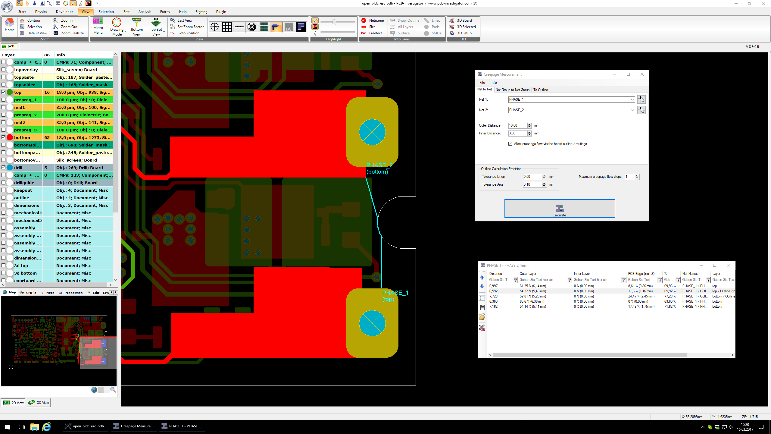
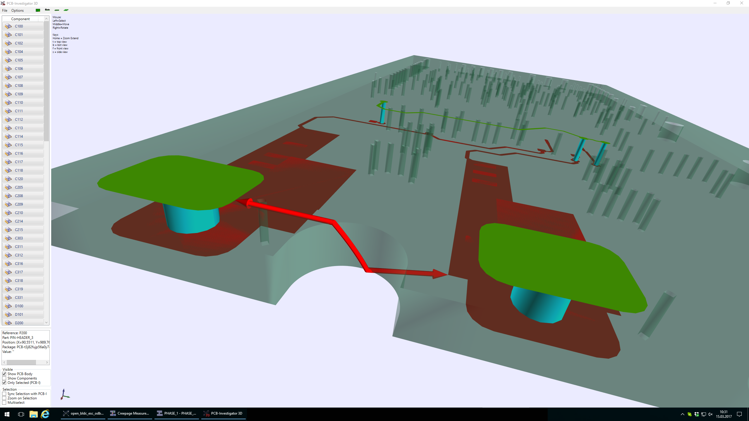
The automatic creepage analysis in PCB-Investigator calculates the shortest distances between conductive parts and to the outer edge of the board. It also takes into account uncoated drill holes (e.g., mounting holes) and indentations – elements that would otherwise require time-consuming manual calculations.
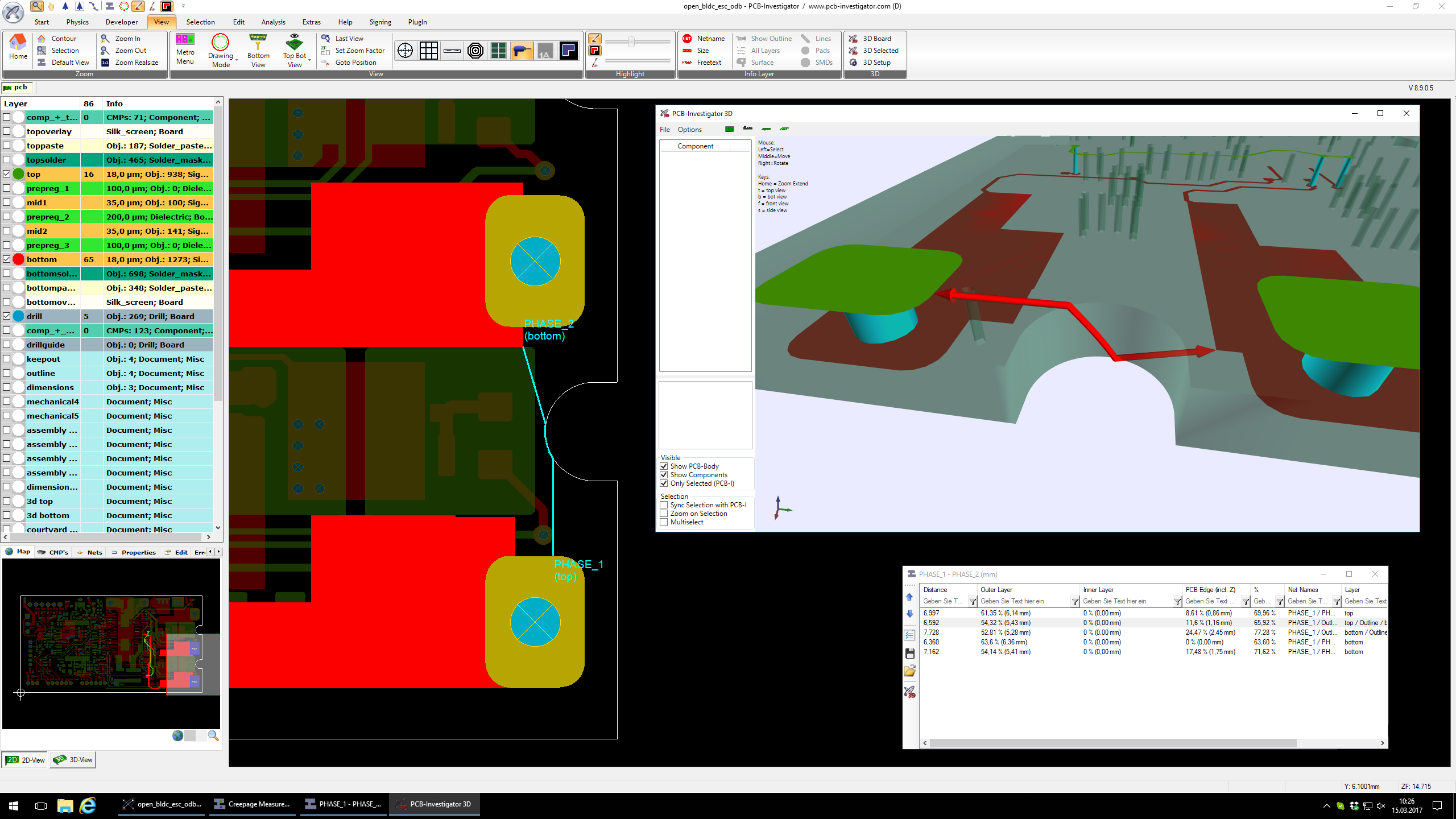
Results are visualized using 3D graphics, helping to avoid common errors found in manual analysis. For example, paths that run at shallow angles around board edges or drill hole rims are measured diagonally, rather than simplified at right angles – a crucial difference, especially in thicker stack-ups.
The evaluation shows the percentage of the required minimum distance achieved for each segment between two contact points. If the total is below 100%, the software highlights the potentially critical path in the results list.
Watch our new video tutorial and contact us to request a free trial version of the software.
Ensure the functional safety of your PCB design – with the Creepage Analysis in PCB-Investigator!

Downloads/Links
» PCBI Manual | Creepage Analysis
Press article:
English: Simplifying Automated Leakage Current Analysis