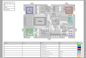

Stencil analysis is a critical step in PCB production
Reliable PCB manufacturing starts long before assembly. One of the most important quality checks is stencil analysis, because solder paste geometry has a direct impact on print quality, assembly yield, and rework risk.
The Stencil Analysis plug-in in PCB-Investigator helps engineers quickly analyze solder paste layers and identify undersized areas. It focuses specifically on the solder paste layers and is directly linked to the stencil thickness, making the review practical and relevant to real manufacturing conditions.
Why this matters for engineers and PCB designers
In many projects, stencil-related issues remain hidden until production reveals them. That often means extra iterations, unexpected defects, or unnecessary delays. A focused analysis step helps teams catch issues earlier and make more confident decisions before release.
For design and manufacturing teams, this means a faster workflow with clearer insight into paste-related risk. It is a simple but effective way to improve manufacturability and production reliability.
When solder paste definition is checked early, production quality becomes much easier to control.
Key benefits of the plug-in
- Fast analysis of solder paste layers
- Detection of undersized areas
- Direct dependency on stencil thickness
- Improved efficiency in manufacturing checks
- Better support for robust PCB production
Conclusion
If stencil quality is part of your DFM or production control workflow, PCB-Investigator’s Stencil Analysis plug-in is worth a look. It helps technical teams assess critical paste structures more efficiently and strengthen production quality from the start.
Learn more and see how stencil analysis can fit into your PCB development process.