
Why a PCB Design Report matters
In PCB development, critical information is often scattered across layout data, analysis results, manufacturing notes, and team communication. The Design Report in PCB-Investigator brings that information together in a structured overview of the most important PCB parameters. The result is less manual follow-up and a clearer technical foundation for everyone involved.
For projects with multiple stakeholders, that matters. A consistent report helps engineering, fabrication, and production stay aligned and reduces the friction that usually comes from missing context or repeated questions.
Automatically generated PCB data
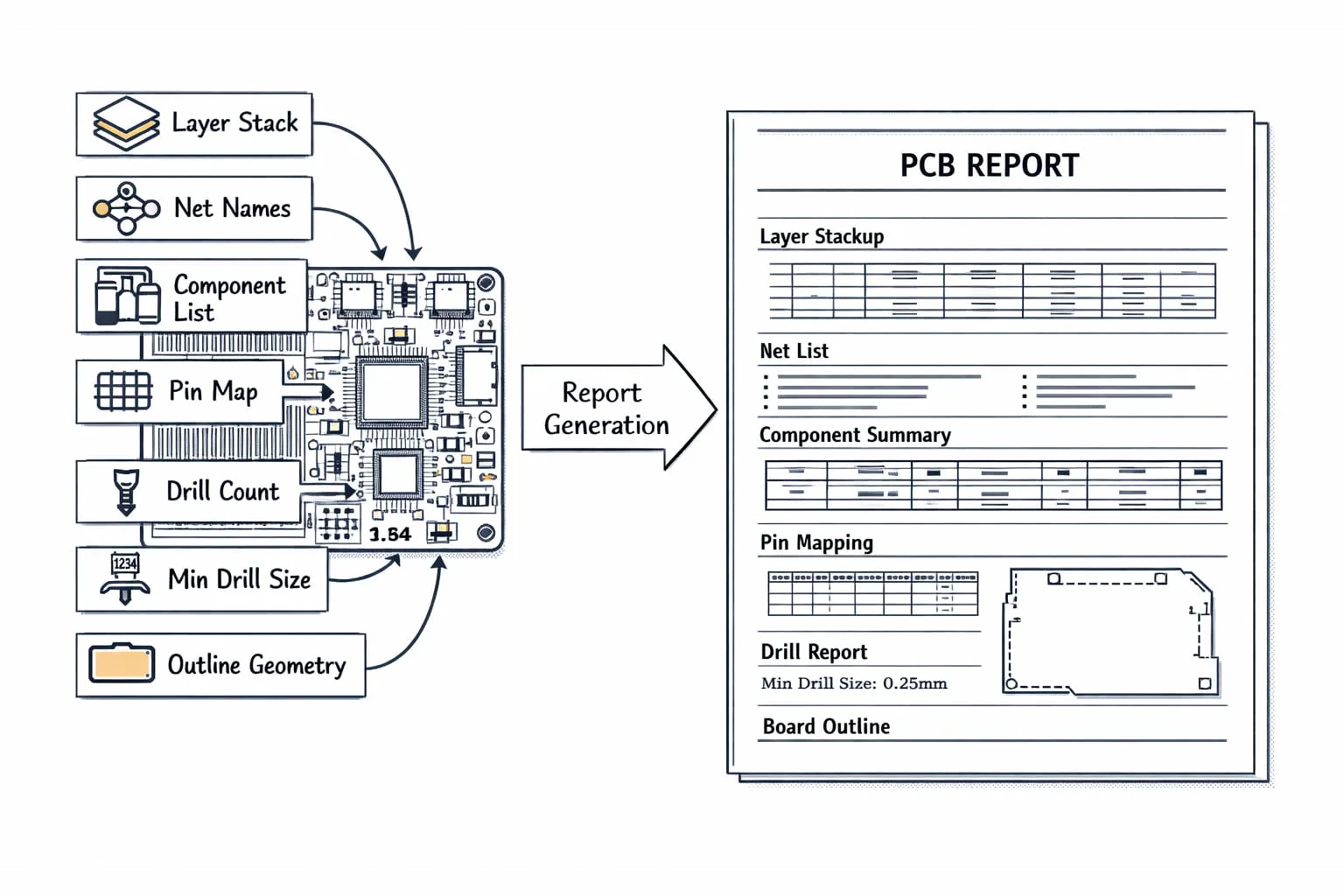
The Design Report captures the key board information automatically and creates an editable Word document. That makes it easy to adapt the report to company-specific formats or add additional details later in the process.
- Number of layers
- Net names
- Components and pins
- Layer stack information
- Board size with outline sketch
- Number of drills and smallest drill size
It can also be enriched with results from other analyses, such as Component Analysis. That turns the report into a practical documentation base for internal review, handoff, and production communication.
A good PCB report does more than document data. It shortens decisions, reduces questions, and improves collaboration across disciplines.
Built for flexible documentation workflows
Because the report is generated as a Word document, it can be edited after creation and exported as RTF when needed. That flexibility makes it easy to fit into different documentation standards and engineering workflows.
If you want to streamline PCB documentation and share technical board data in a cleaner, more consistent way, take a closer look at the Design Report in PCB-Investigator. It is a practical way to reduce overhead and keep projects moving.