Every PCB design contains potential risks that may only become apparent during manufacturing—such as insufficient trace spacing, inadequate annular rings, solder mask clearance issues, or critical drill-to-copper distances. With PCB Investigator’s Bare Board Analysis (DRC), these issues can be identified and corrected before production begins. This helps reduce supplier feedback cycles, lower manufacturing costs, and accelerate time-to-market.
What Does the Bare Board Analysis Check?
The DRC analysis automatically evaluates your design for a wide range of manufacturability-critical parameters, including:
- Trace widths and copper clearances
- Annular rings for vias and drilled holes
- Solder mask clearances
- Copper-to-drill spacing
- Drill diameters and drill-to-drill distances
- Missing or duplicated drill holes
- Exposed copper areas
- Dead-end traces
- Opens and shorts (when a netlist is available)
Step 1: Prepare Your Data
Before starting the analysis, make sure the following prerequisites are met:
- All signal layers must be positive layers.
- The PCB stack-up must be correctly defined.
- Solder mask oversize should already be generated.
- Required attributes for SMD pads, test points, vias, and drill holes must be assigned.
- A netlist is required if you want to perform open/short verification.
A properly prepared dataset ensures accurate results and minimizes false positives.
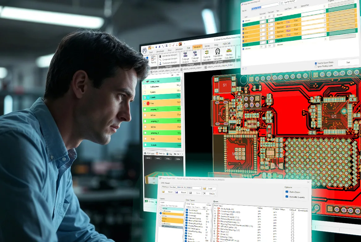
Step 2: Select a Rule Set
PCB Investigator comes with predefined rule sets that can be used immediately. These rule sets can also be customized in the Rule File Manager to match your company standards or PCB supplier requirements.
The Rule File Manager allows you to:
- Create custom rule files
- Import and export rule sets
- Compare different rule configurations
- Define tolerances
- Manage technology-specific limit values
For example, you can maintain one rule set for standard PCB technology and another for HDI designs.
Step 3: Configure Layers and Check Parameters
After selecting a rule set, choose the layers that should be included in the analysis.
For each layer, individual limits can be defined, such as:
- Minimum trace width
- Minimum copper clearance
- Layer-specific rules
- Open/short verification
A helpful indicator is the displayed minimum trace width currently used on each layer. This value can serve as a reference when defining appropriate design limits.
Step 4: Run the Analysis
Click Start to begin the DRC process.
Within seconds, PCB Investigator analyzes the entire design and evaluates numerous criteria across areas such as:
- Outer layers
- Inner layers
- Solder mask
- Silkscreen
- Vias
- Plated through holes (PTH)
- Non-plated through holes (NPTH)
- Microvias
- Buried vias
- Copper foil-dependent rules
A progress bar provides real-time feedback on the analysis status.
Step 5: Review the Results
Once the analysis is complete, all detected violations are displayed in the Result Viewer.
From there, you can:
- Select affected layers
- Filter violations by category
- Inspect individual issues in detail
- Mark critical violations
- Automatically zoom to the error location
The measured value and the configured limit are displayed side by side, making it easy to assess the severity of each violation.
Why DRC Matters
Many manufacturing problems are caused by seemingly minor design violations:
- Copper clearances that are too small can become critical during the etching process.
- Extremely narrow solder mask webs may detach during manufacturing.
- Finer structures often require more advanced and expensive production processes.
Even a single critical violation may force the PCB manufacturer to switch to a more demanding fabrication technology for the entire board. Performing a DRC analysis early in the design process not only improves quality assurance but can also significantly reduce manufacturing costs.
PCB Investigator’s Bare Board Analysis provides a fast and systematic way to identify manufacturability issues before production. With customizable rule sets, comprehensive checking capabilities, and detailed result visualization, engineering and manufacturing teams can ensure that PCB designs meet production requirements early in the development cycle.
For more information, visit our Bare Board Analysis – DRC feature page and the Bare Board Analysis (DRC) section of the PCB Investigator Manual.