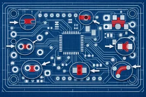
Why stencil analysis matters before production
In PCB manufacturing, the paste printing step can make or break first-pass quality. If apertures are undersized, ratios are off, or the stencil thickness does not match the paste geometry, the result is often poor paste release, bridging, or defects that only appear once the board is already in production.
PCB-Investigator’s Stencil Analysis is designed to catch those issues early. It evaluates only the solder paste layers and uses the stencil thickness as a direct parameter, helping engineers determine whether the solder paste can detach properly from the stencil before fabrication starts.
What the analysis checks
This is not a single-rule lookup. It is a practical set of checks built for real manufacturing workflows, where the goal is to reduce trial-and-error and make paste printing more predictable.
- Aspect Ratio and Area Ratio checks for stencil aperture feasibility
- Solder Paste Type Rules for pad and ball geometry
- Pin Gap Checks to reduce short-circuit risk in tight layouts
- Metal-in-Paste Volume checks for reliable soldering performance
- Squeegee Direction Rules for horizontal and vertical printing paths
- Drill-in-Paste Checks to avoid paste loss through holes
Better visibility, fewer surprises
When paste printing is validated early, the entire assembly process becomes more predictable.
That matters for PCB designers, CAM engineers, and production teams alike. A stencil-aware DFM step can save time on the shop floor, reduce rework, and improve yield without adding unnecessary complexity to the process.
If you want to see how PCB-Investigator supports stencil validation in a technical, production-oriented workflow, take a closer look at the Stencil Analysis feature and compare it with your current process.