
PCB-Investigator Manual for Faster PCB Analysis
A better starting point for PCB-Investigator When you work with complex PCBs, software capability alone is not enough. You also need documentation that helps engineers move quickly from question to…



A better starting point for PCB-Investigator When you work with complex PCBs, software capability alone is not enough. You also need documentation that helps engineers move quickly from question to…

Keep impedance under control in high-speed PCB designsAs data rates rise and edge speeds get faster, controlled impedance becomes a design constraint rather than a nice-to-have. Even small deviations in…

Panelization should not slow down your fabrication flowAnyone responsible for preparing PCB designs for manufacturing knows the pressure: layouts must be arranged into panels, spacing rules must be respected, fiducials…

Training that matches real engineering needsWhether you are just getting started with PCB-Investigator or already use PCB analysis tools every day, the right training makes a measurable difference. It shortens…
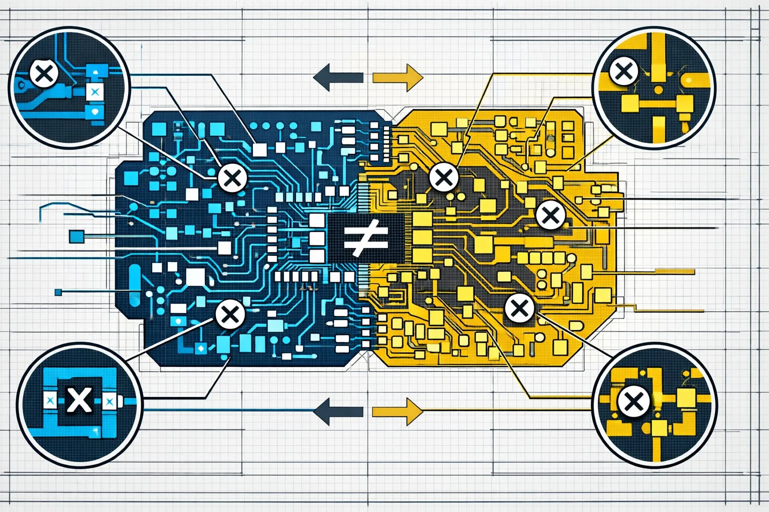
Make PCB change tracking faster and more reliableIn PCB development, change tracking is not a side task. It is a critical part of the workflow, especially during design reviews where…
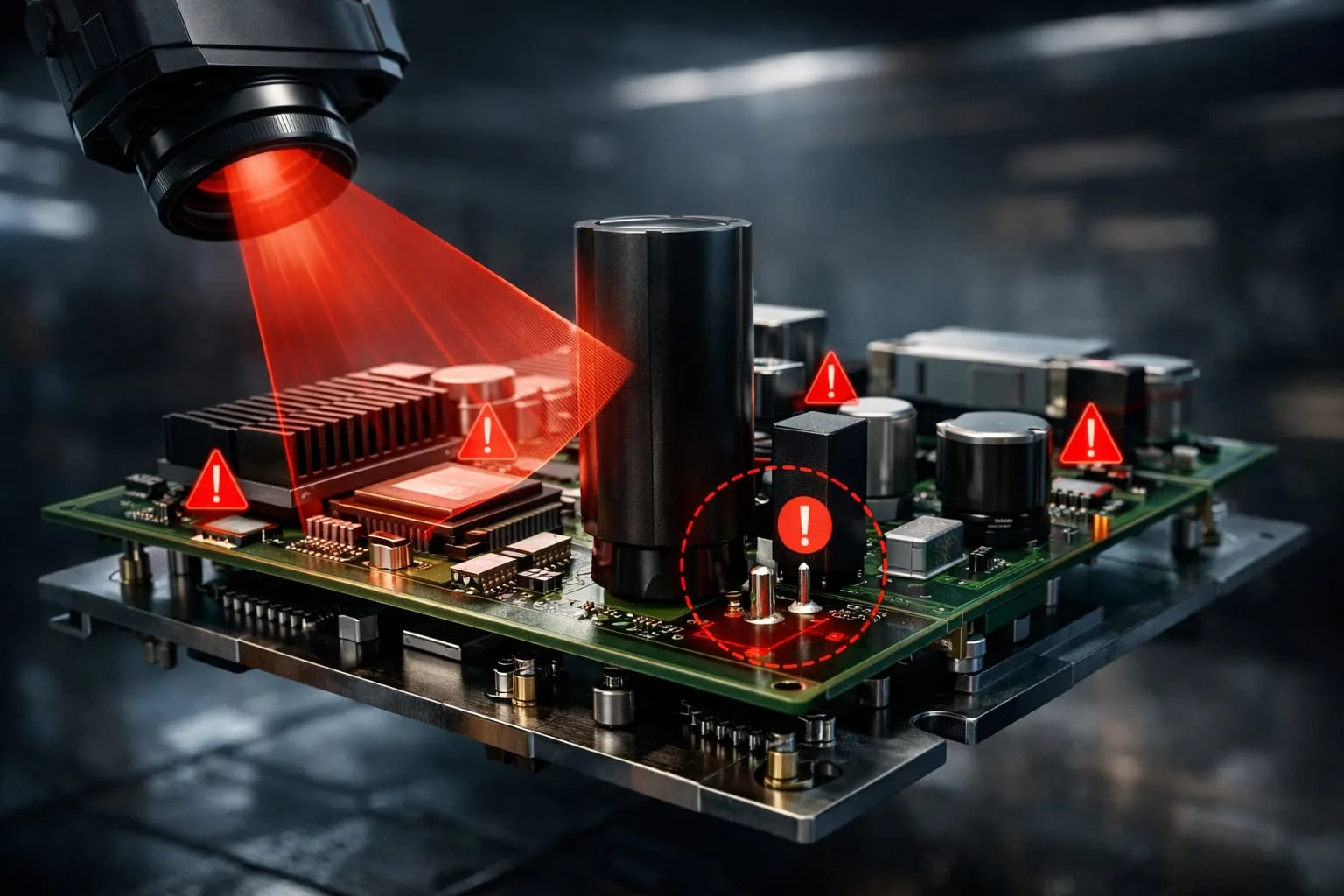
AOI problems usually start in the layoutIf an automated optical inspection system cannot see a pin, the root cause is often not the line—it is the PCB design. Tight component…

PCB-Investigator: 30-Day Free Trial for EngineersChoosing PCB analysis software is never just about features on a product page. The real question is whether the tool fits your engineering workflow, your…

Why Stencil Analysis Matters in PCB DevelopmentIn PCB manufacturing, success is not determined by the circuit layout alone. Just as important is whether the solder paste areas are properly designed…

See power and ground connections instantlyIn complex PCB layouts, quickly identifying the most important supply and ground connections can save a surprising amount of time. The Power Pin Wizard in…
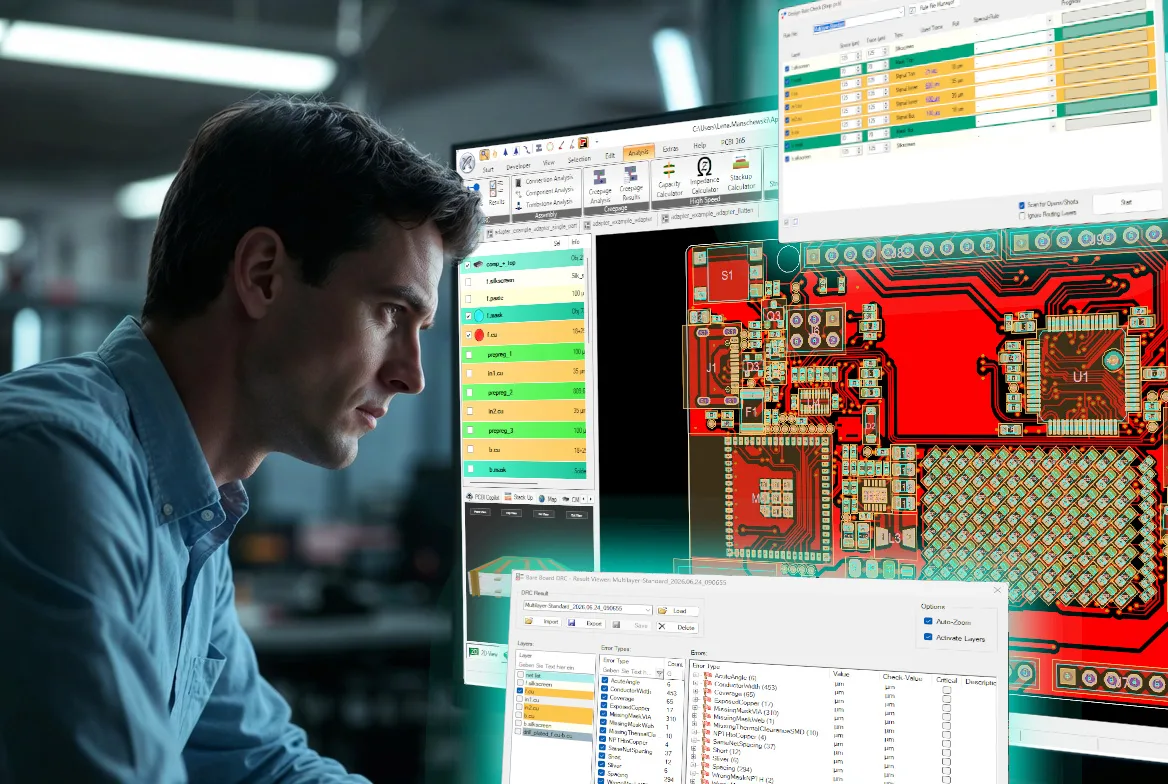
Every PCB design contains potential risks that may only become apparent during manufacturing—such as insufficient trace spacing, inadequate annular rings, solder mask clearance issues, or critical drill-to-copper distances. With PCB…