Why a design report matters in the PCB workflow
In many development projects, time is lost not in the PCB design itself, but in follow-up questions, incomplete documentation, and unclear handoffs between design, fabrication, and production. That is exactly where the Design Report in PCB-Investigator comes in.
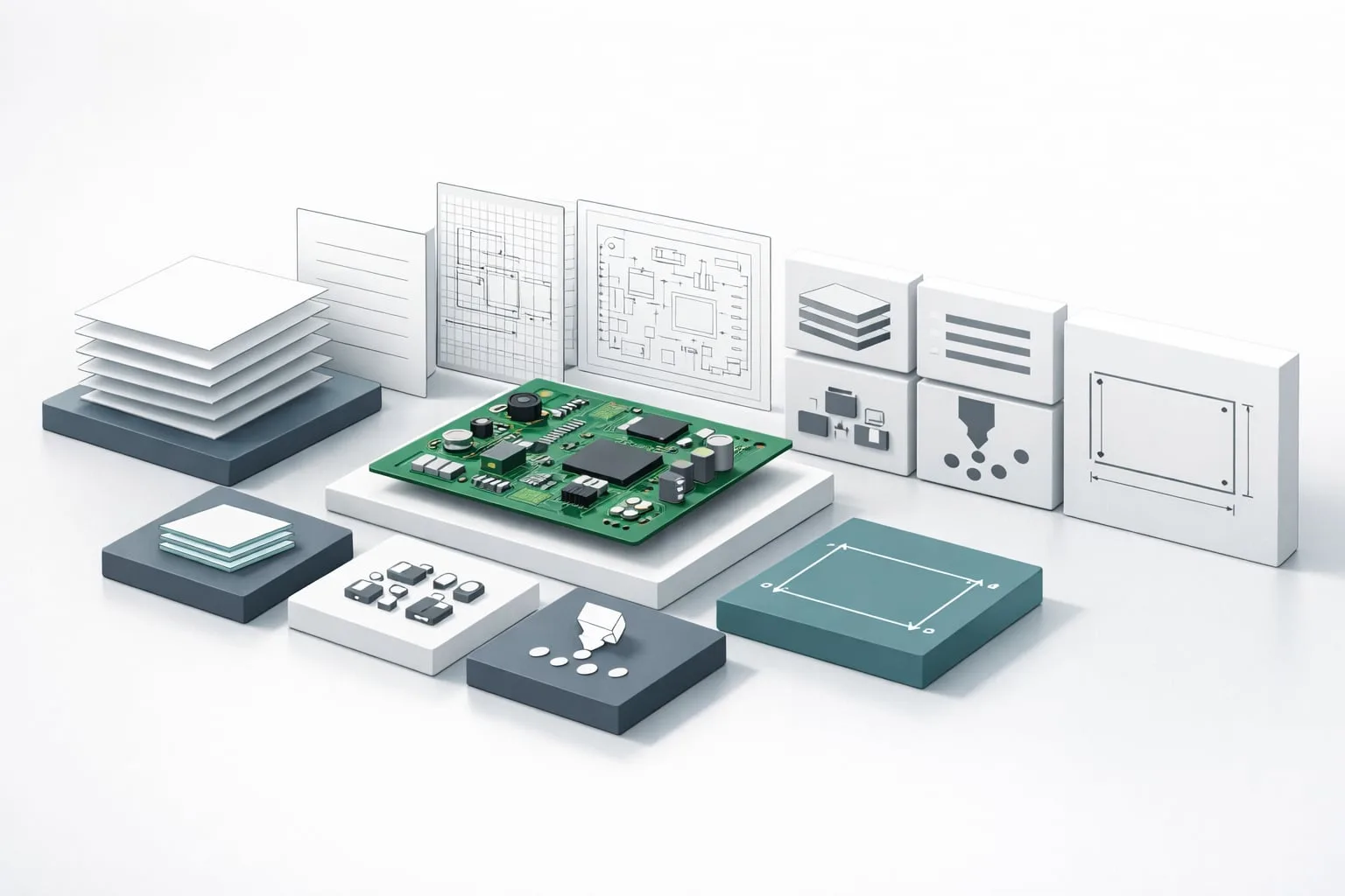
The plug-in automatically creates a structured overview of the most important PCB parameters. This turns scattered design data into a clear, reusable report that makes collaboration across the project much easier.
Automatically generated PCB summary
The Design Report compiles essential information into a Word document that can be edited later and adapted to internal or external requirements, for example by adding company name and address. It can also be exported as RTF.
The report becomes even more powerful when combined with results from other analyses, such as the Component Analysis plug-in. This creates a more complete view of the board and its characteristics.
- Number of steps
- Layer names and net names
- Components and pins
- Layer stackup information
- Board size with outline sketch
- Number of drills and smallest drill size
Clearer communication from design to manufacturing
For engineers, the benefit is simple: less manual documentation effort and fewer repetitive questions during the project. A well-structured design report supports cleaner handoffs, faster alignment, and more transparency in complex PCB projects.
Good documentation is not an extra step. It is a core part of efficient PCB development.
The Design Report is especially valuable for teams that need to present technical information quickly, clearly, and consistently to both internal and external stakeholders.
If you want to streamline your PCB documentation and improve workflow efficiency, take a closer look at the Design Report in PCB-Investigator.
Learn more: https://www.pcb-investigator.com/funktionen/fabrication-tools/design-report/