The best PCB tools do not just answer questions
They help engineers ask the right ones. That is the real difference between a simple viewer and a true analysis platform in electronics development.
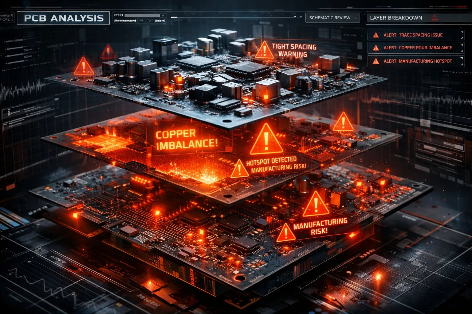
The challenge is usually not a lack of data. It is the sheer amount of information that must be processed before a decision becomes obvious. When a board is opened, critical issues should not have to be hunted down manually.
What should appear immediately
Speed matters, especially in early and mid-stage design reviews. The faster relevant information becomes visible, the earlier teams can act with confidence and reduce downstream risk.
- Critical spacing that may indicate design rule concerns
- Uneven copper distribution that can create thermal or electrical issues
- Manufacturing risks that lead to rework and cost
- Suspicious component placement that affects assembly or signal integrity
A good PCB tool does more than reduce complexity. It makes the next meaningful decision easier to see.
From board viewer to analysis platform
That is why PCB tools are steadily evolving beyond basic visualization. Modern analysis workflows help engineers identify patterns faster, evaluate context more accurately, and prioritize what matters most.
For PCB designers, electronics engineers, and technical decision-makers, that means less time searching and more time making better decisions earlier in the process.
What do you want to see first when you open a PCB? Share your approach with us.