Why creepage analysis matters in modern PCB design
As soon as your design goes above 30 V, creepage is no longer a side topic. Minimum distances between conductive parts become a safety requirement, driven by standards such as DIN EN 60664 / VDE 0110, IPC-2221A, or UL60950-1. In high-voltage designs, overlooking a critical path can quickly turn into a reliability or compliance problem.
The challenge is that creepage is rarely simple to evaluate manually. Board edges, uncoated drill holes, recesses, and diagonal paths all influence the effective distance. Add pollution degree and condensation effects, and what looks safe at first glance may not actually meet the required margin.
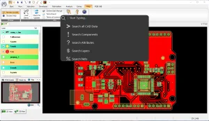
PCB-Investigator automates the difficult part
The Creepage Analysis in PCB-Investigator calculates the shortest distances between conductive parts and to the outer edge of the board. It also considers uncoated holes and board cutouts, reducing the time spent on manual measurements and helping engineers focus on the real risks.
Paths below the required minimum are highlighted clearly in the results list, making critical areas easy to identify.
Visualization in 3D graphics makes the analysis easier to understand and helps prevent common manual errors. This is especially useful in applications such as drive technology and other high-voltage environments, where dielectric breakdown must be avoided with confidence.
What engineering teams gain
- Automatic measurement of critical creepage paths
- Accurate handling of board edges, holes, and recesses
- 3D visualization for faster review and better communication
- Support for compliance-oriented PCB development
- Less manual effort, fewer missed edge cases
If your team is working on safety-critical or high-voltage PCB layouts, take a closer look at the Creepage Analysis in PCB-Investigator. Try the software, watch the tutorial, and see how much faster creepage verification can become in your workflow.